SCANNING PROBE MICROSCOPY GROUP
Laboratory of Semiconductor Physics
Institute of Solid State and Semiconductor Physics
National Academy of Sciences of Belarus
RESEARCH INTERESTS
Main
scientific interest of our group is application of SPM technique
for investigation of surface morphology and electronic properties
of organic semiconductors thin films in close collaboration with
the group of Dr. Artyom Pochtenny (Physics department of Belarussian
State University of Technology). Here
you can find some our results in this area.
The group involved also into research of the our Institute in area
of ion-beam vacuum technologies (magnetic thin films, ion-beam planarization
of optical surfaces, ion-beam metallization in GaN laser technology),
liquid phase epitaxy for single crystals and superconducting films
growth and other.
The SPM group conducts measurements for other organizations. Some
AFM images of crystalline films of complex oxides, photosensitive
semiconductor layers, isolated and native neuron membranes and etc.
can be found here.
HISTORY
OF GROUP
 The
history of scanning probe microscopy (SPM) techniques in our Institute
start from installation of scanning tunneling microscope (STM) of
Advanced Technology Center of MSU in 1992. At the same time Dr.
Valentin Solonovich organized new SPM group that included additional
three peoples. Main objects of investigations at that time were
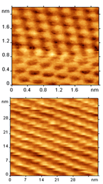
highly oriented pyrolitic graphite (upper STM-image) and Langmuir-Blodgett
films (second STM-image). First doctoral thesis was defended in
May of 1995 by Ms. Lyudmila Kukharenko. In autumn of 1995 Mr. Oleg
Stukalov joined the group as post-graduate student after the completion
of 5 years coa The
history of scanning probe microscopy (SPM) techniques in our Institute
start from installation of scanning tunneling microscope (STM) of
Advanced Technology Center of MSU in 1992. At the same time Dr.
Valentin Solonovich organized new SPM group that included additional
three peoples. Main objects of investigations at that time were
highly oriented pyrolitic graphite (upper STM-image) and Langmuir-Blodgett
films (second STM-image). First doctoral thesis was defended in
May of 1995 by Ms. Lyudmila Kukharenko. In autumn of 1995 Mr. Oleg
Stukalov joined the group as post-graduate student after the completion
of 5 years coa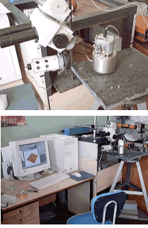 rse
of Radiophysics and Electronics Faculty of Belarussian State University.
In January of 1999 the tragic event occurs – our group leader Dr.
Solonovich is dead on the work place. After this Oleg Stukalov was
appointed as Head of SPM group. In August of 2000 Dr. Kukharenko
leave group for Physics Department of Minsk State Medical University
and now she continues active scientific research in area of atomic
force microscopy (AFM) of living cells. rse
of Radiophysics and Electronics Faculty of Belarussian State University.
In January of 1999 the tragic event occurs – our group leader Dr.
Solonovich is dead on the work place. After this Oleg Stukalov was
appointed as Head of SPM group. In August of 2000 Dr. Kukharenko
leave group for Physics Department of Minsk State Medical University
and now she continues active scientific research in area of atomic
force microscopy (AFM) of living cells.
In March of 1999 under partial financial support of Belarus State
Committee for Science and Technology the Institute purchased new
SPM «FemtoScan-001» with ambient STM head (see photos left) from
Advanced Technology Center of MSU and became first user of the new
line of devices. Then we receive contact mode AFM head in summer
of 2000 and upgrade the SPM device for resonant mode in November
of 2002.
RECENT PUBLICATIONS
1. A.E. Pochtenny, A.V. Misevich, I.G. Yaminsky, M.O. Gallyamov,
V.K. Solonovich, O.M. Stukalov. Nanostructural sensor films of copper
phthalocyanine and their polymer composites. In “Physics, Chemistry
and Application of Nanostructures” (Eds. V. E. Borisenko, S. V.
Gaponenko, V. S. Gurin.– World Scientific, Singapore, 1999) – pp.
221–224.
2. О.М. Stukalov, А.V. Misevich, А.Е. Pochtenny, М.О. Gallyamov,
I.V. Yaminsky. Atomic force microscopy of thin sensor films of copper
phthalocyanine–polysterene composite / Surface Investigation, 2001,
V. 16, pp. 1819-1822.
3. A. V. Misevich, A. E. Pochtenny, I.P. Ilyushonok, O.M. Stukalov.
Structural, electrical and gas sensing properties of copper phthalocyanine
nanoparticles in polystyrene. In “Physics, Chemistry and Application
of Nanostructures” (Eds. V. E. Borisenko, S. V. Gaponenko, V. S.
Gurin.– World Scientific, Singapore, 2001).– pp. 321–325.
4. A.E. Pochtenny, O.M. Stukalov, V.L. Mironov, D.G. Volgunov, A.G.
Biryukov. Photoassisted scanning tunneling microscopy/spectroscopy
of copper and lead phthalocyanine thin films // Physics of Low-Dimensional
Structures.– 2001.– Vol. 3/4.– P.109–116.
5. Stukalov О.М., Misevich A.V., Pochtenny A.Е. Influence of thickness,
composition, substrate and annealing conditions on morphology of
nanostructured copper phthalocyanine based films // Physics of Low-Dimensional
Structures.– 2001.– Vol. 3/4.– P.205–215.
6. A.I. Stognij, N.N. Novitski, O.M. Stukalov. Ion beam polished
nanodimensional relief on the surface of optical materials // Technical
Physics Letters, 2002, Vol. 28, # 1, pp. 17-20.
7. O.M. Stukalov. Application of atomic force microscopy for DNA
and protein biochips development. In "Frontiers of Multifunctional
Nanosystems" (Eds. Buzanaeva E.V., Scharff P. - Kluwer Academic
Publishers, Dordrecht, 2002, 500 pages), pp. 331-340.
8. Stukalov О.М., Pochtenny A.Е. V.L. Mironov, S.V. Gaponov, D.G.
Volgunov. Application of photoassisted STM for investigation of
local photoconductivity of thin phthalocyanine films // Physics
of Low Dimensional Structures, 2002, #5-6, pp. 121-127.
9. O.M. Stukalov, A.E. Pochtenny. Influence of local resistance
on STM characterization of phthalocyanine films. Physics of Low-dimensional
Structures, 2002, #5-6, pp. 129-135.
10. A.I. Stognij, N.N. Novitski, O.M. Stukalov. A method for monitoring
thicknesses of nanodimensional bilayer film structures. Technical
Physics Letters, 2003, Vol. 29, # 2, pp. 147-150.
11. A.I. Stognij, N.N. Novitski, O.M. Stukalov. A method for evaluating
the thickness of ultrathin films. Instruments and Experimental Techniques,
2003, #3, in print.
12. A.V. Misevich, A.E. Pochtenny, О.М. Stukalov, M.O. Gallyamov,
I.V. Yaminsky. Atomic Force Microscopy of Sensor Films Containing
Copper Phthalocyanine. Probe Microscopy, 2003, in print.
13. V. Pankov, О. Stukalov, S. Smolenchuk, A. Bartholdson, O. Babushkin.
Growth of BaFe12O19 thin films using reactive diffusion. Journal
of Crystal Growth, 2003, in print.
14. A. N. Lappo, A. V. Misevich, A. E. Pochtenny, O. M. Stukalov,
G. K. Zhavnerko. Correlation of morphology and electrical conduction
in nanostructured perylene pigment films. In “Physics, Chemistry
and Application of Nanostructures” (Eds. V. E. Borisenko, S. V.
Gaponenko, V. S. Gurin.– World Scientific, Singapore, 2003).– in
print.
CONTACT INFORMATION
Dr. Oleg Stukalov (the group leader)
Institute of Solid State and Semiconductor Physics
National Academy of Sciences of Belarus
P. Brovki 17, 220072 Minsk, Belarus
Tel.: (+375)-(17)-284-11-82
Fax: (+375)-(17)-284-12-49
e-mail: nanom@ifttp.bas-net.by
ICQ# 14487276
|